Nexwafe technology review. Nexwafe is developing a next-generation PV silicon technology called the EpiWafer process, growing standalone silicon wafers onto mono-crystalline seed wafers, with no need to slice ingots and surrender 30-50% of the PV silicon as ‘kerf’ sawdust.
This should improve the manufacturing efficiency, module efficiency and energy intensity of solar PV, and possibly also the costs. Silicon efficiency also matters more in the solar industry, to deflate future costs, after improved passivation has decreased the relative contribution of surface losses.
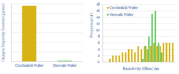
Data from the patent library shows how the resulting wafer can have 98% lower levels of oxygen impurities, and 4-5x narrower distributions of dopant distributions. 1.1% total efficiency gains are also targeted through a combination of optimizing wafer width and dopant distributions.
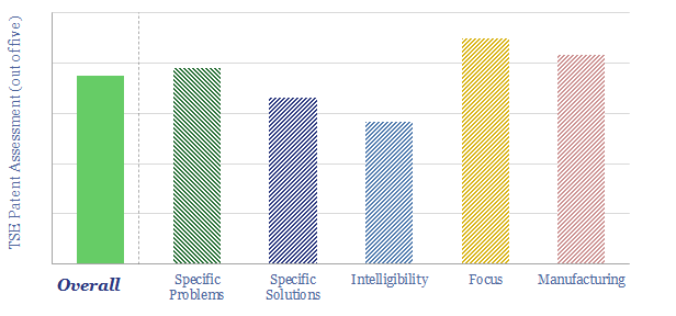
Our Nexwafe technology review found 60 filings and re-filings of 8 separate patents. We conclude that many underlying aspects of Nexwafe’s PV silicon ambitions are locked up with high-quality patents. However, our main surprise was the simplicity of the process, which is both a blessing and a curse (details in the data-file).
Company. Nexwafe spun out from Germany’s Fraunhofer Institute in 2015, has c40 employees, closed a €32M financing round in October-2021, lead by Reliance and including Saudi Aramco Energy Ventures.