MOSFETs are fast-acting digital switches, used to transform electricity, across new energies and digital devices. MOSFET power losses are built up from first principles in this data-file, averaging 2% per MOSFET, with a range of 1-10% depending on voltage, switching, on resistance, operating temperature and reverse recovery charges.
MOSFETs and other power transistors matter, as they are the basis for solar inverters, wind converters, electric vehicle traction inverters, AC-DC rectifiers, other DC-DC converters, the power supplies to data-servers, AI and other digital devices.
Transistors are digital switches made of semiconductor materials, which allow one circuit to control another. Our overview of semiconductors explains how a transistor works, from first principles, by depicting a bipolar junction transistor (BJT), which is driven by current.
However, it is better to control a transistor using voltage than current. Ambient electrical fields induce currents that can cause current-driven transistors to misfire. Hence MOSFETs and IGBTs are driven by voltage.
MOSFETs were invented at Bell Labs in 1959 and are now the most used power semiconductor device in the world. Something like 2 x 10^22 transistors have been produced across human history by 2023.
MOSFETs: how do they work?
We are sorry to say it, but it is simply not possible to understand how a MOSFET works, without a basic understanding of voltage, current, conduction band electrons, valence band holes, N-type semiconductor, P-type semiconductor and Fermi Levels. Do not despair! To help decision-makers understand these concepts, we have written an overview of semiconductors and an overview of electricity.
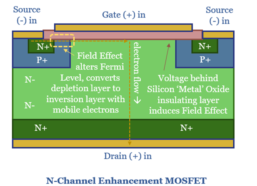
MOSFET stands for Metal Oxide Semiconductor Field Effect Transistor. Actually this is something of a misnomer. The eponymous ‘metal oxide’ is referring to an oxide of silicon metal, or in other words, a highly pure layer of silicon dioxide. It is oxidized to create an insulating layer. In turn, the reason for creating this insulating layer is so that a Field Effect can be induced by a potential difference (voltage) across the gate.
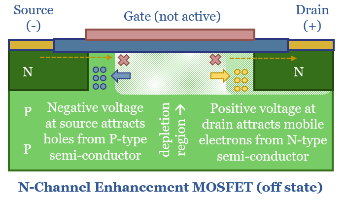
Why can’t current flow through a MOSFET in the off-state? A simplified diagram of an N-channel enhancement MOSFET is shown below. Ordinarily, electrons cannot flow from the source to the drain, due to the PN junction between the body and the drain, which is effectively a reverse-biased diode. A negative voltage at source draws in the mobile holes from the P-type semiconductor. A positive voltage at the drain attracts the mobile electrons in the N-type layer. And this creates a depletion zone where no current can flow, just like in any other diode.
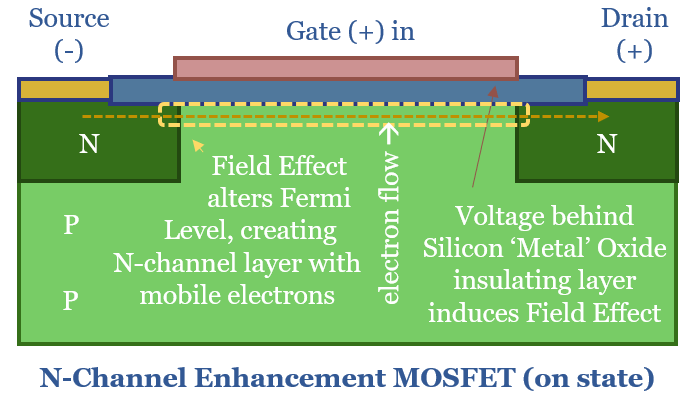
How can current flow through a MOSFET in the on-state? The ‘Field Effect’ occurs when a positive voltage is applied to the gate, raising the Fermi level of the P-type semiconductor. Remember the Fermi Level is the energy level likely to be exceeded by 50% of electrons. A large enough voltage raises the Fermi Level above the lower bound of the conduction band. Suddenly there is a sea of mobile electrons, forming an N-channel, so that electrons can flow from source to drain.
What power losses in a MOSFET?
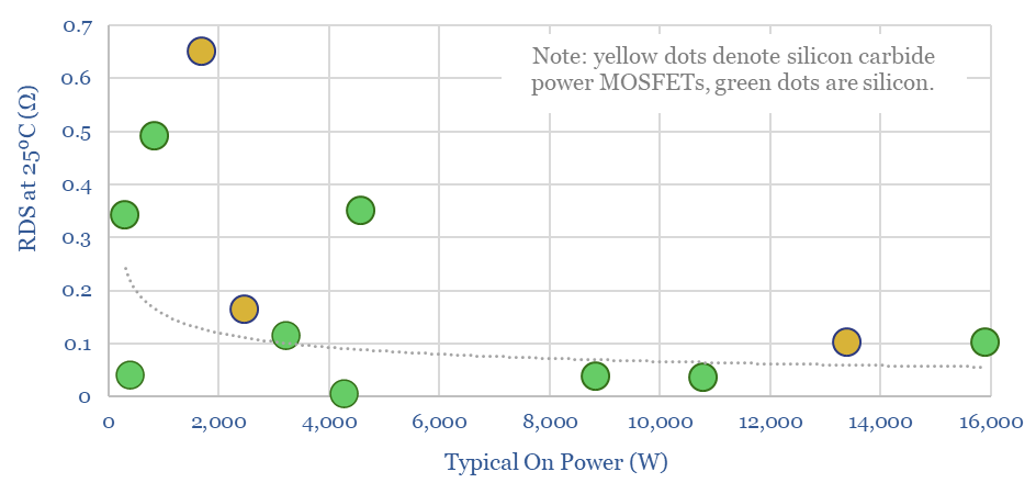
Resistive losses occur when a current flows through a semiconductor, proportional to the on-resistance of the semiconductor, and a square function of the current. The on resistance of different MOSFETs is typically in the range of 0.1-0.6 Ohms, at power ratings of 1-20kW, based on data-sheets from leading manufacturer, Infineon (as profiled in our screen of SiC and MOSFET companies).
Hence a better depiction of an N-channel enhancement MOFSET follows below. In the chart above, the N-channel through the P-layer is very long and thin, which is going to result in high resistance. Hence in the chart below, the NPN junction is slim-lined, and the on resistance from source to drain is going to be lower, which helps efficiency.
Raising voltage is also going to reduce I2R conduction losses, because less current is flowing. However, voltage is limited by a MOSFET’s breakdown voltage. Above this level, the PN junction will fail to block the flow from source to drain, and the MOSFET will be destroyed (avalanche breakdown). The voltage ratings of different MOSFETs are tabulated in our data-file. A clear advantage for silicon carbide power MOSFETs is their higher breakdown voltage, which allows them to be operated at higher voltages across the board, reducing conductive losses.
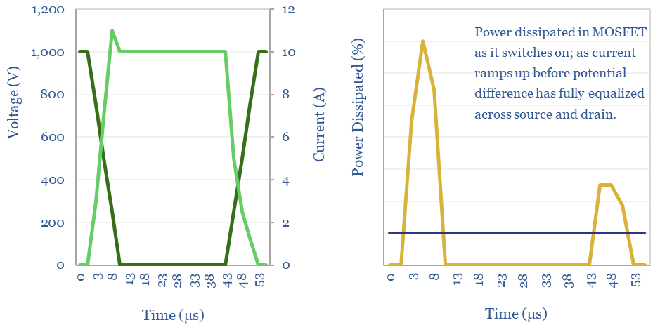
Switching losses are also incurred whenever a MOSFET turns on or off. When the MOSFET is off, there is a large potential difference (voltage) between the source and the drain. When the MOSFET turns on, current flows in while the voltage is still high, which dissipates power. And then the voltage falls when current flow is high, which dissipates power. The same effect happens in reverse when the MOSFET is switched off. These losses add up, as the pulse width modulation in an inverter will often exceed 20kHz frequency. And the latest computer chips run with a clock speed in the GHz. Minimizing switching losses is the rationale for soft switching, being progressed by companies such as Hillcrest.
A reverse recovery loss is also incurred by a MOSFET, because every time the MOSFET switches on, the body diode needs to be inverted from reverse bias to forward bias. This physically requires moving charge carriers, or in other words, requires flowing a current. The reverse recovery loss can often be the largest single loss on a MOSFET.
Transistors: IGBTs vs MOSFETs?
IGBTs stand for Integrated Gate Bipolar Transistors, which is another transistor design that has been heavily used in solar, wind, electric vehicles and other new energies applications.
An IGBT is effectively a MOSFET coupled with a Bipolar Junction Transistor, to improve the current controlling ability.
IGBTs are generally more expensive than MOSFETs, and can handle higher currents at lower losses. However when switching speeds are high (above 20kHz), MOSFETs have lower losses than IGBTs, because IGBTs have slow turn off speeds with higher tail currents.
Finally, in the past, it was suggested that IGBTs performed better than MOFSETs above breakdown voltages of 400V, although this is now more nuanced, as there are many high-performance MOSFETs with voltages in the range of 600-2,000 V.
The very highest voltage IGBTs and MOSFET modules we have seen are in the range of 6-12 kV. This explains why so much of new energies requires generating at low-medium voltage then using transformers to step up the power for transmission; or conversely using transformers to step down the voltage for manipulation via power electronics modules.
Formulae for the losses in a power MOSFET?
This data-file aims to calculate the power losses of a power MOSFET from first principles, covering I2R conduction losses, voltage drops across the diode, switching losses and reverse recovery losses, so that important numbers can be stress tested.
Generally, the losses through a MOSFET will range from 1-10%, with a base case of 2% per MOSFET. These numbers consist of conduction losses, voltage drops across the diode layer, switching losses and reverse recovery charges.
Losses add. Many circuit designs contain multiple MOSFETs, or layers of MOSFETs and IGBTs (example below). Roughly, flowing power through 6 MOSFETs, each at c2% losses, explains why the EV fast-charging topology depicted below might have losses in the range of 10-20%.
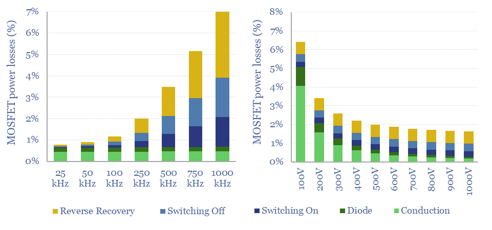
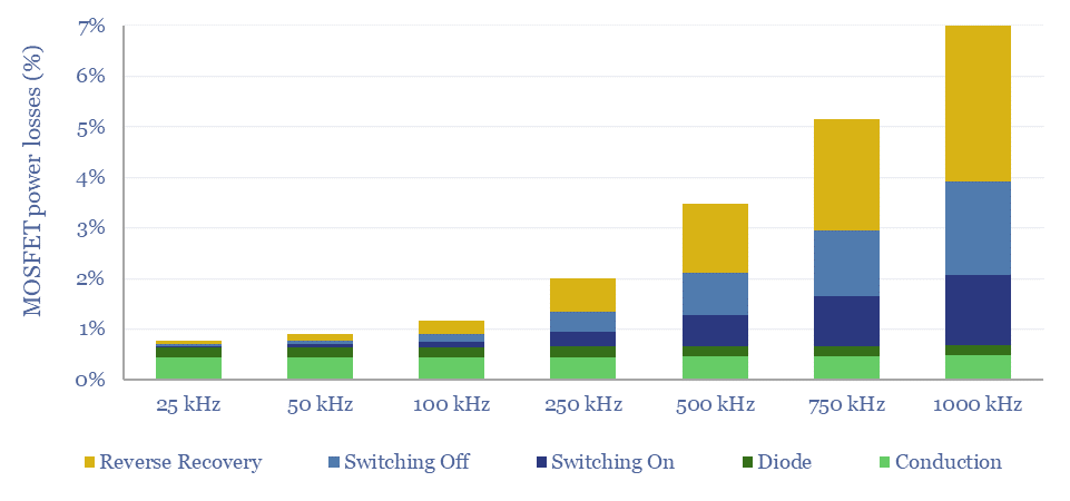
Power losses in a MOSFET rise as a function of higher switching speeds, as calculated in the data-file, shown in the chart below, and for the reasons stated above. High switching speeds produce a higher quality power signal, but are also more energetically demanding.
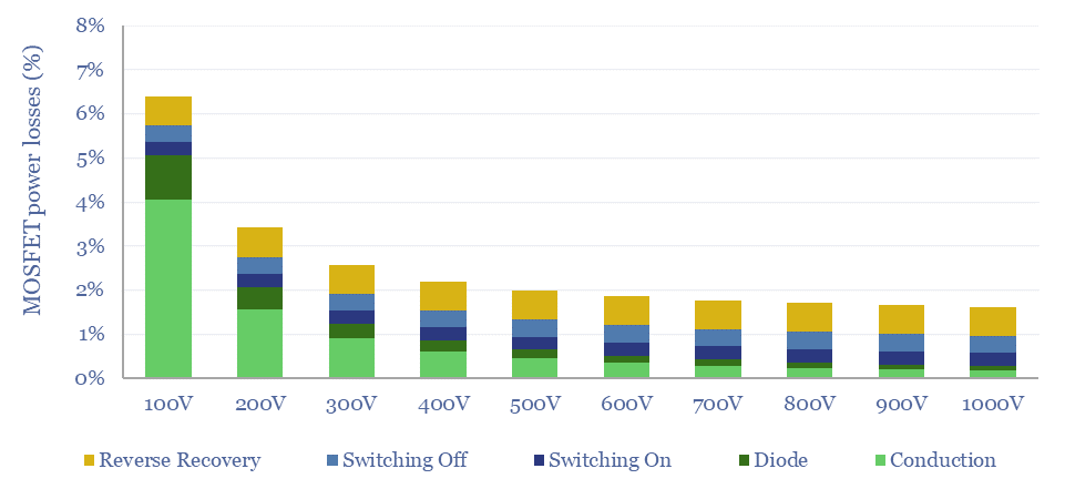
Power losses in a MOSFET fall as a function of Voltage, as calculated in the data-file, shown in the chart below, and for the reasons stated above. Although lower voltage MOSFETs face less electrically demanding conditions and are less expensive.
Overall, our model is intended as a simple, 30-line calculator to compute the likely power flow, electricity use and losses in a MOSFET. This should enable decision makers to ballpark the loss rates of MOSFETs, and power electronic devices containing them.
However, interaction effects are severe. Drain current, breakdown voltage, gate voltage, temperature, on resistance, reverse recovery charges and all of the switching times depend on one-another. Hence for specific engineering of MOSFETs it is better to consult data-sheets.
Semiconductor manufacturers also stood out in our recent review of market concentration versus operating margins.