Semiconductors underpin solar panels, electric vehicles and electronics. Hence this 20-page note aims to explain semiconductor physics from first principles: their conductivity and resistance, their use in devices, plus implications for materials value chains and the energy transition itself?
Semiconductors are a true workhorse of the energy transition, especially if solar efficiency doubles again, to enable AI, and for electrification.
A salty observation might be that commentators love to make sweeping statements about all of these initiatives, without really understanding how semiconductors work or “what is a Fermi Level?”.
We have read several textbooks and technical papers into semiconductor physics. The purpose of this note is to distil the underlying theory, into 20 concise pages, which are relevant to semiconductor devices, materials value chains and energy transition itself.
The resistance of metals is explained on pages 2-3. From first principles, why does the copper used in electronic devices have a conductivity of 5.9 x 10^5 S/cm and a resistivity of 1.7 x 10^-6 Ωcm.
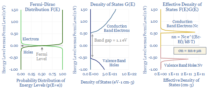
The resistance of semiconductors is different from the resistance of metals, because of the complexity of their charge carriers. Pages 4-7 cover the physics: the Pauli Exclusion Principle, the Fermi-Dirac distribution, the Density of States, the Boltzmann constant, bandgaps, and key formulas for semiconductor conductivity (calculations here).
Semiconductors are really not very good conductors. This is why a solar panel contains more copper than silicon and always will (page 8).
Doping can be used to achieve different conductivity and resistance profiles in semiconductors, introducing precise amounts of pentavalent impurities (N-type) or trivalent impurities (P-type). How does doping change the physics? How much dopant is introduced? Why has the solar industry shifted from P-type cells to N-type cells? (please see pages 9-10).
Semiconductor theory allows you to understand PN junctions (page 11), light emitting diodes (page 12), solar modules (and their inevitable progress towards being the world’s lowest cost energy supply source, pages 13-14), transistors (page 15), their combination into MOSFETs, inverters, and converters (page 16) and the rise of wide bandgap technologies such as silicon carbide (SiC) (page 17).
The value chain for silicon wafers is summarized on pages 19-20, covering silica mining, silicon metal, polysilicon production, polysilicon markets, and 20 companies across this entire value chain.